forked from torvalds/linux
-
Notifications
You must be signed in to change notification settings - Fork 2
LANCOM NWAPP2
J. Neuschäfer edited this page Dec 4, 2024
·
6 revisions
aka. L-321agn Wireless (R2), L-322agn dual Wireless
- LANCOM console port (RS-232 over mini-DIN 8-pin)
- 1x Gbit Ethernet, PoE enabled, +1 unpopulated port
- 12 V DC
- 1x mPCIe slot (for WLAN), +1 unpopulated slot
Top side:
- U1: Freescale MPC8314E SoC - powerpc 32-bit, PowerQUICC II, e300 core
- U5/6: 2x NANYA NT5TU32M16EC-AC, 512Mb DDR2 SDRAM (128 MiB total)
- U22: Atheros AR8035-A Ethernet PHY
- U21: SIPEX SP3238ECA RS-232 Transciever
- U11: P16C557, PCIe® 2.0 Clock Generator
- U14/15: 2x HC 595A PHCE, Onsemi MC74HC595A: 8-Bit Serial-Input/Serial or Parallel-Output Shift Register with Latched 3-State Outputs
- U20: TI SNx4HC165 8-bit parrallel-load shit register (marked
HC165 3H6H701) - U16: TI CD54HC221 high-speed CMOS logic dual monostable multivibrator with reset (marked
HJ221 53K) - U19: TI SNx4HC74 dual D-type positive-edge-triggered flip-flops with clear/preset (marked
HC74 3C9Y501) - U17: ADI ADM708 low-cost microprocessor supervisory circuit (NOTE: the watchdog is not present in this variant)
Bottom side:
- U7: Micron 29F2G08ABAEA, 2Gb ONFI NAND flash (256 MiB)
- U10: TI SNx4LVC08A Quad 2-input AND gates (marked
LC08A 53K) - U34: TI SNx4HC4060 14-stage async binary counter/oscillator (marked
550380K HC4060)- acts as watchdog timer
- using a RC oscillator. R1=
40C(?), R2=1Ω → 1.75 kHz - the output of pin 1, 2, or 3 is selected by 10kΩ resistor placement (reset pulse?), goes to both sides of JP5
- 4.6s period (toggles every 2.3s), 1.8V
- T7 brings it to 3.6V
On a device which inexplicably forgot its firmware:
WDG:
@C@
memory test:  1 2 3 4 5  OK

Found primary and mirror bbt

NO VALID FIRMWARE!

# FLASHROM-Upload
| LANCOM L-321agn Wireless (R2)
| Copyright (C) LANCOM Systems
| Ver. 4.00.0001 / 12052014 / 132211

Start Xmodem Upload
...

Receive Error

Upload aborted
Successful boot
WDG:
@C@
memory test:  1 2 3 4 5  OK

Found primary and mirror bbt

Start firmware #1

ZLoader running..............................................................................................................................................................................................................................................................................................................................................................................................................................................................................................................................................................................................................................................................................................................................................................................................................................................................................................................................................................................................................................................................................................................................................................................................................................................................................................................................................................................................................................................................................
Outband-115200 Bit/s OK
Pressing enter after boot starts the LCOS shell.
- Booting with JP3 (
DBG) bridged drops you into a little shell. - Shorting JP5 to ground disables the watchdog.
LANCOM Systems Boot-Loader log
WATCHDOG DISABLED
Found primary and mirror bbt

NO VALID FIRMWARE!
----------------------------------------------
LANCOM Systems Boot-Loader
Version 4.00.0001 / 12052014 / 132211
Copyright (C) 2012 LANCOM Systems GmbH
 Vendor: LANCOM Systems
 Oem:
 Device: LANCOM L-321agn Wireless (R2)
 HwId:   NWAPP2
HW-Release: H, PLD-Release: --
CCB clock 133MHz, Core clock 400MHz, VCO clock 267MHz, DDR clock 133MHz LBC Clock 33MHz
Reset cause: 0

Debug-Adapter: absent
phystop: 08000000, ramfirm_end: 08000000
Minimum FW/LD version is 8.82/3.41
Active Firmware: 2
Bitrate = 115200.8N1
V<adr>/I/R/G/B/S/U/D/e/f/t/H/?>

Adr = 00000000, Len=0x80
00000000:  00 00 00 00 00 00 00 00  00 00 00 00 00 00 00 00 | ................
00000010:  00 00 00 00 00 00 00 00  00 00 00 00 00 00 00 00 | ................
00000020:  00 00 00 00 00 00 00 00  00 01 F9 E0 00 00 00 00 | ................
00000030:  00 10 00 00 00 10 73 30  00 00 8A 30 48 00 89 F4 | ......s0...0H...
00000040:  00 02 ED 10 00 00 00 04  00 00 00 00 00 00 00 01 | ................
00000050:  FE 00 00 00 FE 02 ED 10  FE 00 00 00 00 00 00 00 | ................
00000060:  34 2E 30 30 3F 00 00 00  00 FF 22 C1 00 00 00 02 | 4.00?.....".....
00000070:  00 02 ED 10 42 00 00 00  60 00 00 00 60 00 00 00 | ....B...`...`...

V<adr>/I/R/G/B/S/U/D/e/f/t/H/?>

Monitor help page
-----------------
 V<adr>  : Dump memory addresses <adr>
 G       : Start active firmware
 I       : Version Info
 U0,U1   : Upload file to Flash-ROM by XMODEM-/CRC
 R       : Reboot (Warmstart)

 Bx      : Modify outband bitrate

 E ...*  : Erase menu       * = action required
 F ...   : Firmware menu
 T ...   : Test menu
Memory can be dumped by repeatedly issuing V commands.
The test (T) menu has a few more peek/poke commands, as well as lspci.
| address | length | description |
|---|---|---|
00000000 |
128 MiB | RAM |
e0000000 |
1 MiB | MMIO (relocated by IMMRBAR) |
| address | length | description |
|---|---|---|
00000000 |
00008000 |
loader 1 |
00008000 |
00078000 |
loader 2 |
00080000 |
00f80000 |
loader spare (empty) |
01000000 |
0f000000 |
YAFFS file system |
- Internal watchdog: write
0x556c,0xaa39to0xe000020e- This one isn't actually enabled at boot. Linux stays alive without it.
- External watchdog: Toggle GPIO 18 (mask 0x2000) by writing to GPDAT (
0xe0000c08)
The board has multiple bi-colored LEDs (A=red + B=green). They seem to be controlled via SPI.
| U14 | pin | U15 |
|---|---|---|
| LED1A | A | LED6A |
| B | ||
| LED3A | C | LED7A |
| D | LED8A | |
| LED4A | E | LED18A |
| F | ||
| LED5A | G | LED19A |
| H |
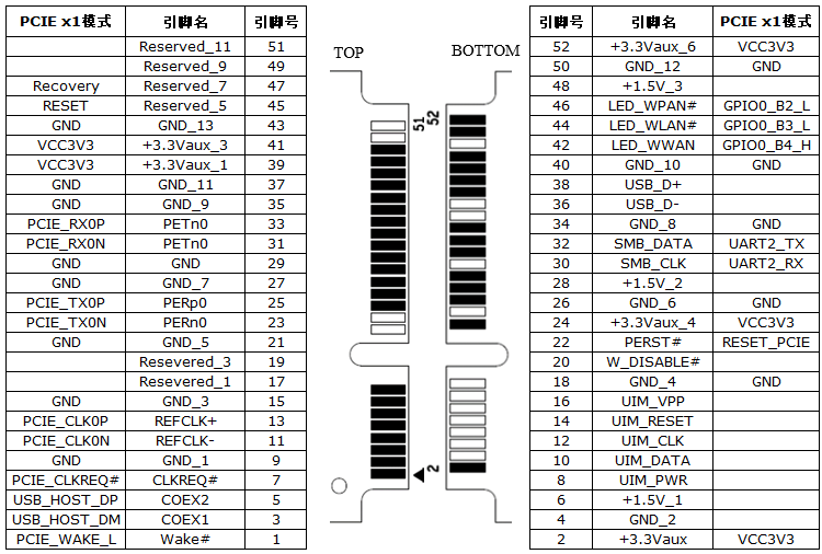
In L-321 devices, only one of the two mini-PCIe slots is populated.
- Soldering the slot itself is fairly straight-forward, but make sure to test for continuity and shorts.
- By default, the 3.3V rail (pin 2) isn't active.
- Populate L22, which brings 3.3V
- Populate C293, C294, C295, as well as C291, C292 to stabilize the 3.3V supply
- Add some sort of mounting holes (CN19/13 or CN20/15)
